PCB design2L · 4LAltium Designer
2 to 4 layer PCB design.
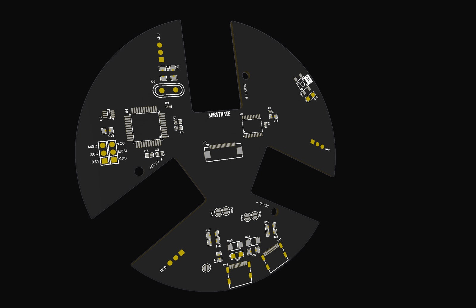
P01 Tri-Servo Controller BaseDesigned in Altium Designer →
01 / Work
Selected boards.
Power, embedded, RF, motion and sensing boards. Open any board for the full write-up.
02 / Capabilities
What goes into a board.
The full design path for two-layer and four-layer boards, in Altium Designer.
- C.01
Schematic capture
The circuit drawn as a clean, readable schematic that serves as the single reference for the layout.
- C.02
2-layer layout and routing
Placement and routing on two copper layers, for simpler and cost-sensitive boards.
- C.03
4-layer layout and routing
Placement and routing on four copper layers, for denser boards that need inner layers.
- C.04
Design-rule and manufacturability checks
DRC and DFM checks before release, so the board can be built as drawn.
- C.05
Manufacturing outputs
Gerber or ODB++, drill files, bill of materials and pick-and-place files.
TopL1
Core
BottomL2
TopL1
Prepreg
Inner 1L2
Core
Inner 2L3
Prepreg
BottomL4
03 / Process
Four steps, one board.
- Step 01
Brief
You share what the board needs to do, its size limits and any parts already chosen.
- Step 02
Schematic
The circuit is captured as a schematic and reviewed with you before layout starts.
- Step 03
Layout
Parts are placed and routed on two or four layers, then checked against the design rules.
- Step 04
Manufacturing files
You receive the files a fabricator and assembler need to build the board.
04 / Contact
Start a board.
Send a short description of your project by email or WhatsApp.
